Playstation PU-18 8MB RAM Modification


Parts and tools required
- A PlayStation with a PU-18 motherboard that uses 4 RAM chips
- Replacement RAM – 4 x KM48V2105AJ-6
- Soldering iron with selection of bits
- Thin wire
- No. 2 point Philips screwdriver
- Solder
- Fine point wire cutters
- Rework flux
- Scalpel or Ex-Acto knife
Technical details
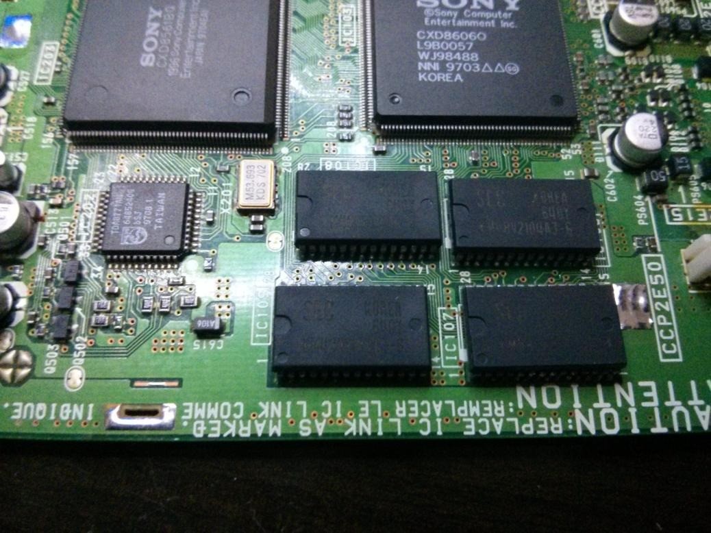
The original RAM subsystem consists of 4 Samsung KM48V514BJ-6 EDO DRAMs – these are 2 megabit devices organized as 512kB x 8 with 3.3V I/O, 1024 rows and 512 columns – they require 1024 refresh cycles every 16ms. Like most DRAMs, they have a multiplexed address bus where you have to apply the row address (10 bits in this case), assert a strobe (RAS/) then put the column address (9 bits) and assert CAS/ - the connections between the CPU and the RAM are conventional, except that the A8 line on the RAM chip is wired to the pin on the CPU that you would expect to be A11. The CPU A8 and A10 pins are not connected at all.
There is also a difference between the memory controller used in the original CPU (used on the PU-7, early PU-8 and DTL-H2000) and the newer one (used on everything else) – which is that the original CPU output 2 RAS/ lines (only one used), 1 CAS/ line, and 4 WE/ lines (one for each byte) – the newer one outputs 2 RAS/ lines (still only one is used), 1 WE/ line and separate CAS/ lines for each byte. This has few practical implications, as long as you are aware of it, but it does mean that the old style board requires slightly more rework. This (along with the better CD servo) was the reason that the PU-18 was chosen as the first test platform.
The replacement RAM is using the same chips that were installed on the DTL-H2000 – these are Samsung KM48V2104AJ-6 devices – also EDO, but arranged as 2MB x 8 with 2048 column addresses and 1024 row addresses. They also require more refresh cycles (2048), but over 32ms, so the actual refresh rate is identical. They are also connected with all the address pins lined up between the device and the CPU. There are a few other pinout differences, too – these are best illustrated using the pinout diagrams.
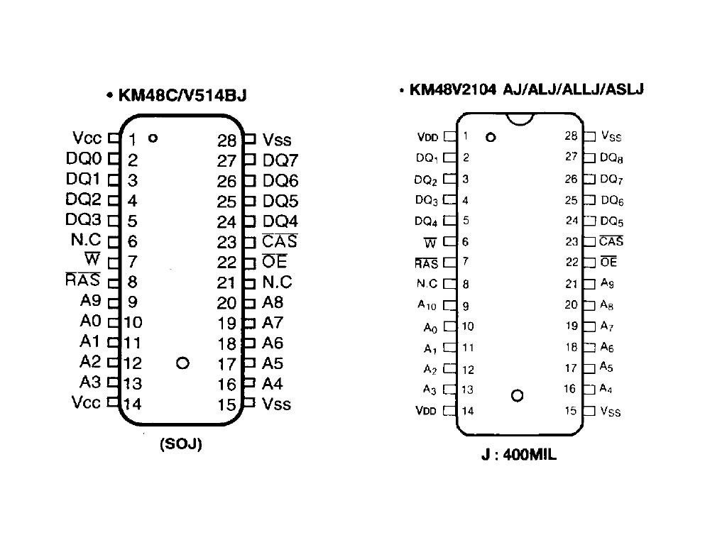

- Pin 6 was no connection, and is now WR/
- Pin 7 was WR/ and is now RAS/
- Pin 8 was RAS/ and is now no connection
- Pin 9 was A9 and is now A10
- Pin 21 was no connection, is now A9.
Pin 20 also needs to be reconnected, not because it has changed function on the chip but because it needs to be moved from the A11 address line to A8. As a result, there are 4 existing circuits that need to be cut, and a total of 6 connections that have to be made.
Disassembly
Unscrew the 6 black No. 2 Philips screws on the underside of the console and remove the upper cover.
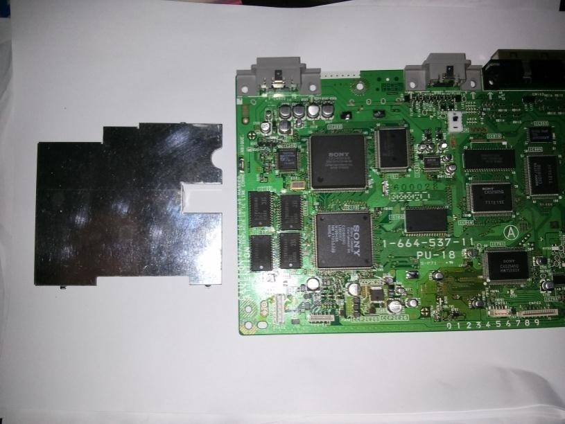
Carefully remove the FPC and 4-pin connector connecting the optical drive unit to the motherboard –remove the optical drive unit. Unplug the 5 pin connector coming from the PSU and the FPC from the controller assembly. Remove 3 screws from upper PCB shield and then the PCB shield.
The PCB is secured into the case with 5 screws – remove these and then the PCB.
Rework Instructions
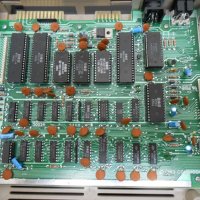
Start by removing the shielding cover soldered to the left side of the board over the RAM and CPU area.

Now remove the 4 RAM chips – if you have a hot air station, this is the easiest method. If not, the safest method is to cut all the pins and then remove the pins individually. If you have some other method you like, then use that.
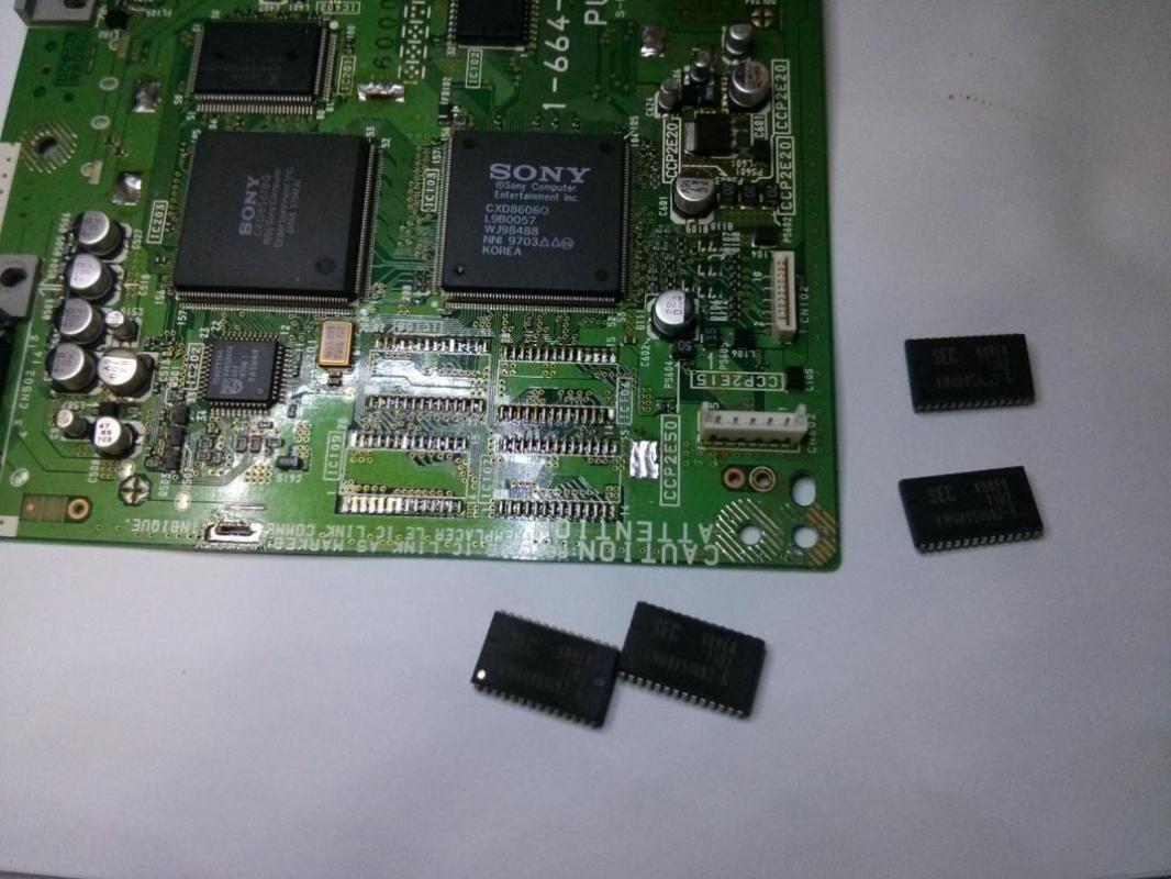

Next, clean up the pads on the board – I just used a large chisel point tip and rework flux.
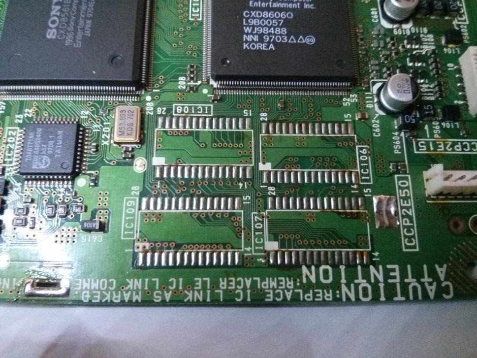

Now solder the replacement RAM chips in position

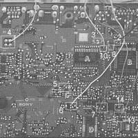
The next stages are done on the back of the board, in the area underneath the RAM and CPU.
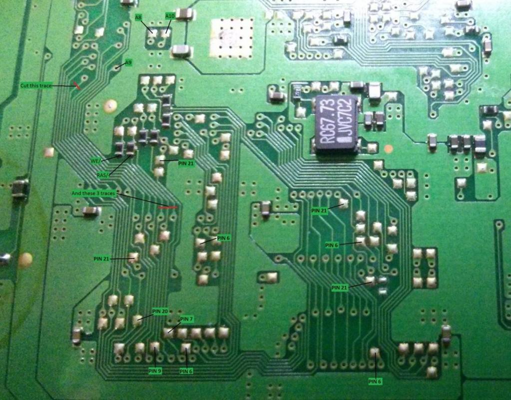

First of all, cut the traces in the places marked with a red line in the photograph – there are two cuts, and a total of 4 traces need to be isolated. You then need to make the following connections:
- All 4 “Pin 6” points should be wired up to the WE/ point
- All 4 “Pin 21” points should be wired up to the via marked A9 (you may have to remove the solder resist)
- Pin 7 has to wire to the RAS/ point
- Pin 9 has to wire to the A10 point
- Pin 20 has to wire to the A8 point
Note that WE/ and CAS/ are the ends of SMT resistors, so use a fine-tip iron.
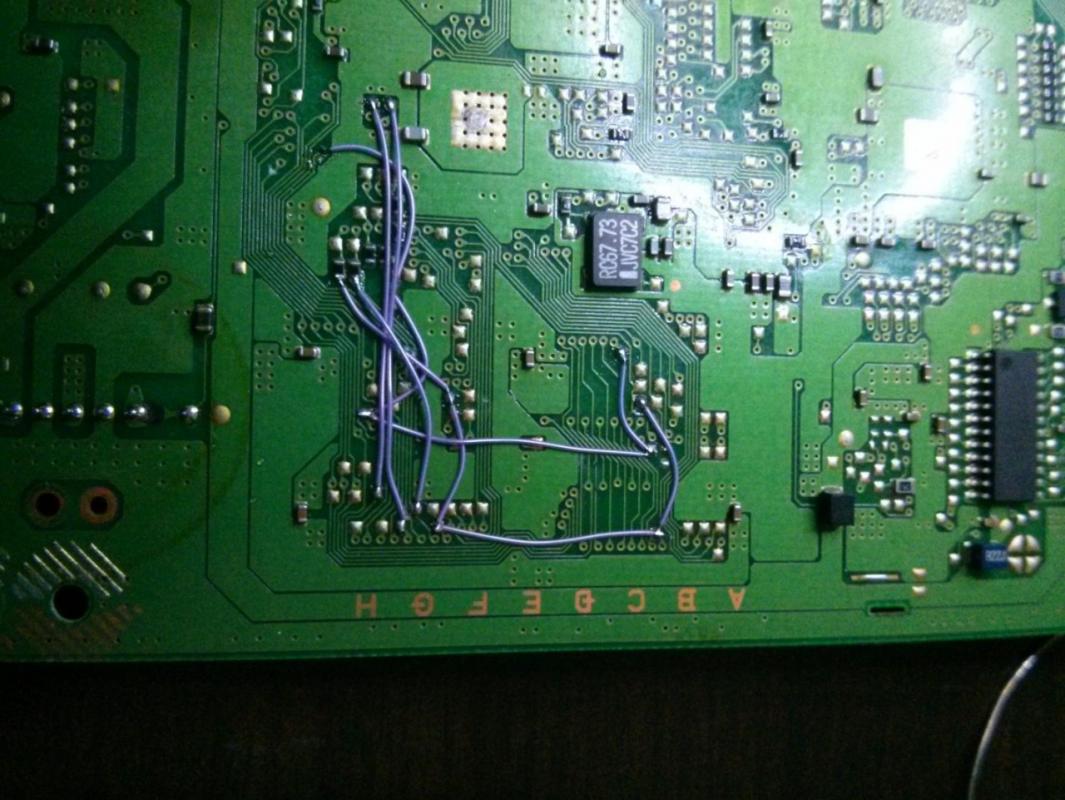
When you have finished, it should look something like this

Before you start putting the shields back on, do a visual inspection, and verify that the machine boots and run games normally – if it doesn’t work, then check for bad connections, solder shorts, miswired pins, etc. This mod does not require any software support – the retail BIOS sets up an 8MB space for the RAM, and the logic to address the larger RAM seems to already be in the BIOS.
Reassembly
Proceed in the opposite order from disassembly – solder the PCB shield back in place, screw the PCB back into the case (5 screws), replace the upper shield (3 screws), plug the optical pickup, power supply and controller ports back into the board and finally reattach the upper cover.
You now have a 8MB retail PSX – I have also written a little memory test utility that you can use to verify that the RAM is working correctly.